Considering Electric interface at 2...
02
05
Considering Electric interface at 200G, power consumption required for communication will be halved
Consider the Electrical interface side on the assumption that 200G will pass
Two times before, last time, I mainly talked about Optical, but the electrical interface side was also examined.
This is a simple story, and if it is 100G x 8, transmission and reception are 8 lanes each, so this is "QSFP-DD" (or "QSFP-DD800" introduced here) or "OSFP" introduced here. I can handle it.
This is also the case when the optical interface side is 200G x 4 instead of 100G x 8. If you install 2: 1 Gearbox, you can convert it to 200G x 4 inside the module (it is still in the stage of considering feasibility, so power consumption and cost at the time of mounting are not considered), so it is not so difficult.

The problem is when aiming for 1.6T after that. With a configuration that requires 200G x 8, it is impossible to say that the Electrical interface side is 100G x 16.
In the first place, there is no such module standard, and even if it is developed, it is essential that it be as large as CFP2 / CFP8, and if it is not good, it may be as large as CFP as shown below, and of course it is the current QSFP / OSFP. Compatibility with system modules will also be lost. It would be difficult to expand the signal terminals of the QSFP / OSPF system to 16 lanes in each direction.
Dimensional drawing of the module shown on the CFP MSA web page.By the way, this height is doubled if you do not have a heat sink.Incidentally, 100G x 8 is not easy either. In the case of a two-stage stack module in the QSFP-DD800, the tricky standard of pulling out the signal directly in the upper stage was standardized, which is the flip side of the fact that it is difficult to handle.
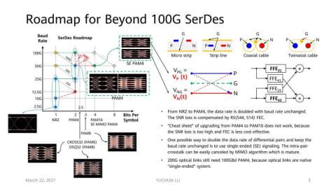
Exploded view of the two-tiered module of QSFP-DD800. Aside from the lower connector, the upper wiring is amazing. Source: Figure 3-5 of QSFP-DD800 Specification Rev 1.0Returning to the story, that's why we also considered Electrical Signaling of 200G per lane. The presentation "Considerations on 200G per lane PAM Signaling" has been presented by Huawei's Yuchun Lu and Yan Zhuang.
As a prerequisite, it is a major premise to pass a 200G (212.5Gbps to be exact) signal.
Except for "Compatible with 100G and slower speed link", all the issues seem to have a high threshold.By the way, the story explained at the beginning is based on the module interface (AUI) in mind, but in reality, the connection between dies in the LSI inside the module and the wiring inside the module are also in view. On the contrary, Backplane / Copper Interconnect systems such as KR and CR are out of consideration here (although I am afraid that KR / CR is completely included in Power Efficiency).
Probably, regarding KR / CR, the distance is too long with the same standard and it is difficult to reach it as it is, so it seems that it can not be realized without adding additional FEC etc., but in the first place it is possible to realize a standard with wiring less than 1 foot. It is obvious that the standard of 1m order will not be established without it, and as the basis of the KR / CR standard, it seems that we want to first formulate a wiring standard of less than 1ft or cm order.


