The structure of the Turing core an...
10
03
The structure of the Turing core and the calculation method of the mysterious index "RTX-OPS" are also revealed! The whole picture of the GeForce RTX 20 series gradually becoming visible
If you have the "holy grail" of the CG world called "real-time ray tracing", you can easily implement expressions that were difficult with the conventional "rasterization method". NVIDIA, which created the "GeForce RTX 20 series" based on the new architecture "Turing", was the first to work on this holy grail.
In August, the RTX 20 series was unveiled for the first time at the special event "GeForce Gaming Celebration" held in Cologne, Germany. I was able to hear stories on a deeper level.
Information was lifted today (September 14th), so in the previous article "Understanding the GeForce RTX 20 series, which worked on the holy grail of the CG world 'real-time ray tracing'" [Part 1] [Part 2] Report I would like to delve into the technical aspects of the RTX 20 series, including what I couldn't do and what I found out later.
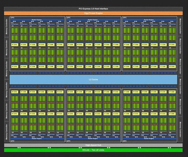
Full-scale "TU102" core configuration
First, let's look at the structure of the Turing core. The core of "GeForce RTX 2080 Ti" is "TU102", "GeForce RTX 2080" is "TU104", and "GeForce RTX 2070" is "TU106", each with a different design.
Given that both the Pascal generation GTX 1080 and 1070 were products born from the same GT104, and the product with the ending "6" was for the middle range (GTX 1060 in this case), GeForce If the RTX 2060 comes out, will it be "TU107"?
First, let's check the "full scale" TU102 diagram. First, 64 CUDA cores, 8 Tensor cores, and 1 RT core are arranged per SM (Streaming Multiprocessor). The number of CUDA cores has been halved from the Pascal generation, but it can be read that it is an advanced form of Volta from the fact that two of the arithmetic machines for FP32 and INT32 are counted as one, and the presence of eight Tensor cores.
The circuitry inside the Turing die. Although it is not clearly stated which part is which function, it can be considered that the upper and lower center is L2 cache, and the pattern that can be seen innumerably on the left and right is SM.
The biggest improvement is the splitting of the FP32 and INT32 calculators. In game shader processing, FP32 and INT32 processing are mixed. In the architecture up to the Pascal generation, when executing INT32 processing in SM, even if there is an idle CUDA core, it was not possible to make FP32 processing.
However, in Turing (and Volta), by separating the FP32 and INT32 data paths, both processing can be handled in parallel. How the INT32 line is used differs depending on the game, but NVIDIA says that it can expect a throughput improvement of 10 to 50%.
By the way, Volta had 32 units for FP64 per SM, but Turing has 2 units per SM, and the throughput is 1/32 of FP32 in terms of computing performance. NVIDIA explains that reducing FP64 "allows any program to run FP64 code correctly."
The biggest difference between the Volta generation and the Turing generation is that each SM unit is equipped with the core technology of the RTX 20 series, the RT core. I will explain the role of this RT core in detail later.
Block diagram of full spec TU102. The "Quadro RTX 8000" announced prior to the RTX 20 series has such a structure.
Block diagram of RTX 2080 Ti based on official specs (imagined by the author). It is speculated that 4 SMs and 1 memory controller are disabled. Disabled circuit locations may vary.
Structure of Turing generation SM. The CUDA cores are divided into FP32 and INT32, each with 16 + 2 Tensor cores forming 4 small clusters with a scheduler. It is operated as SM by adding RT core etc. there. Although the FP64 calculator is omitted in the figure, two units are built into each SM. A meaningful icon is drawn in the background of the RT core, but I will explain it later.
Structure of Volta generation SM. By dividing FP32 and INT32, it is from this generation that both operations can be processed in parallel. Note that Turing is not completely higher than Volta, such as having 32 FP64 processors and slightly more L1 data cache (also used as shared memory) than Turing.
Structure of Pascal generation SM. The CUDA core of this generation can also perform INT32 operations, but the basic design is specialized for FP32 operations. In addition, the L1 cache and shared memory shared by SM units are independent.
By separating the FP32 and INT32 arithmetic units, it becomes possible to perform parallel processing of the two types of operations. The figure above shows how much INT32 processing is in each PC game title when the ratio of FP32 processing is set to 1. The dark green part in the graph is the merit obtained by being able to perform parallel processing with FP32.
In the Turing generation, the cache hierarchy was also heavily modified. Pascal had adopted a structure of 48KB of L1 cache in SM, 96KB of shared memory separately, and 3MB of L2 cache shared by the entire GPU. In Turing, on the other hand, the L1 cache and shared memory is 96KB in the SM, and the 6MB L2 cache is shared by the entire GPU.
With this new shared memory, the L1 cache can be expanded up to 64KB, increasing the hit rate to the L1 cache. In addition, the latency of the L1 cache is reduced, and the bandwidth to the load & store unit in SM is also thicker than before. Depending on the design of the game engine, NVIDIA claims that this L1 cache change will greatly contribute to performance.
Difference in cache structure between Pascal generation and Turing generation. In addition to doubling L2, Turing adopts a new shared memory that combines L1 cache and shared memory. It is not clear whether the volume is a flexible variable type or a mode switching type, but in typical game processing, L1 is often set to 64KB and shared memory to 32KB. It is said that the shared memory is often used at 64 KB.
By combining the L1 cache and shared memory, the throughput of the L1 cache in particular is improved and the latency is reduced. Although it depends on the processing on the game side, it claims that the performance of the shader in the actual game will increase by about 1.6 times (more than double for VRMark).


\" to check personal information leaks - S -MAX")


